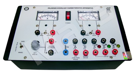
PN/Zener Diode/ LED Characteristics Apparatus (ME543)
Forward and Reverse bias V-I characteristics of PN junction diode, Zener diode& forward bias characteristics of a LED.
Product Overview
Forward and Reverse bias V-I characteristics of PN junction diode, Zener diode& forward bias characteristics of a LED.
Forward and Reverse bias V-I characteristics of
PN junction diode, Zener diode& forward bias
characteristics of a LED.
Outputvoltage (Regulated): 0-3V/30V DC (Selectable)
Meters(Analog): 65mm round 0-3V/30V DC(Dual Range),
0-100uA / 10mA DC (Dual Range).
Housed in PVC cabinet, symbol diagram printed,
connections of various components (PN Junction Diode
0A 79, Zener diode 5.1V, LED's (Red, Green & Yellow )),
For more details please refer datasheet.
Technical Specifications
Forward and Reverse bias V-I characteristics of
PN junction diode, Zener diode& forward bias
characteristics of a LED.
Outputvoltage (Regulated): 0-3V/30V DC (Selectable)
Meters(Analog): 65mm round 0-3V/30V DC(Dual Range),
0-100uA / 10mA DC (Dual Range).
Housed in PVC cabinet, symbol diagram printed,
connections of various components (PN Junction Diode
0A 79, Zener diode 5.1V, LED's (Red, Green & Yellow )),
For more details please refer datasheet.
Talk To Our Technical Experts
Related Products
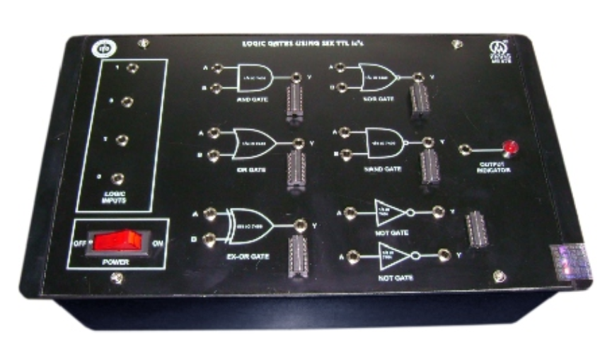
RTLLogic Gates (ME 678)
RTLBasic Logic Gate Apparatus has been designed to verify the truth table for ‘OR’Gate, ‘AND’Gate, ‘NOT’Gate, ‘NOR’Gate, and ‘NAND’Gate using RTL log
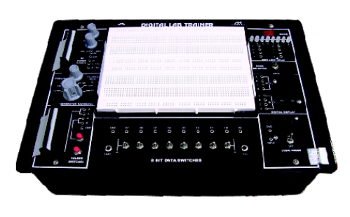
Digital Lab Trainer (Bread Board Model) (ME 1154)
Advanced lab trainer for students to perform more than 50 experiments of digital electronics
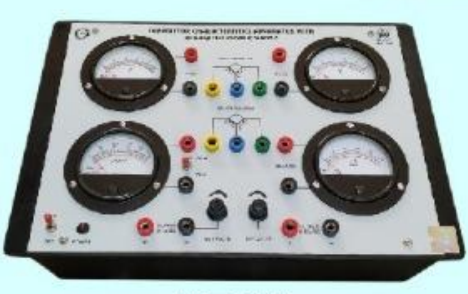
Transistor Characteristics Apparatus (ME 533)
Plot the input, output and transfer characteristics of PNP & NPN transistors in common emitter & common base configuration.
Biasing of Transistor As Class 'A' Amplifier (ME 623)
Biasing of Transistor as Class