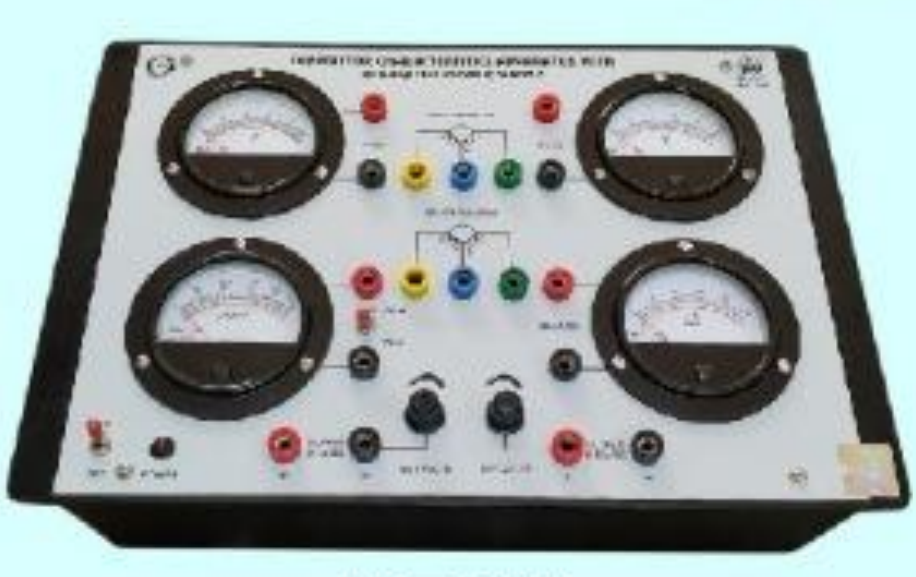
Transistor Characteristics Apparatus (ME 533)
Plot the input, output and transfer characteristics of PNP & NPN transistors in common emitter & common base configuration.
Product Overview
Plot the input, output and transfer characteristics of PNP & NPN transistors in common emitter & common base configuration.
Plot the input, output and transfer characteristics
of a PNP & NPN transistor in common emitter & common
base configuration.
Inbuilt Variable DC Regulated Power Supplies
Output voltages : 0-1VDC, 0-10VDC
On Board Analog Moving Coil Meters (60mm x 35mm )
Voltmeter: 0-1VDC, 0-10VDC
Ammeter: 0-50mADC, 0-250uADC/0-50mADC (Dual range)
Transistors provided
PNP: CK 100
NPN: CL 100
For more details please refer datasheet.
Technical Specifications
Plot the input, output and transfer characteristics
of a PNP & NPN transistor in common emitter & common
base configuration.
Inbuilt Variable DC Regulated Power Supplies
Output voltages : 0-1VDC, 0-10VDC
On Board Analog Moving Coil Meters (60mm x 35mm )
Voltmeter: 0-1VDC, 0-10VDC
Ammeter: 0-50mADC, 0-250uADC/0-50mADC (Dual range)
Transistors provided
PNP: CK 100
NPN: CL 100
For more details please refer datasheet.
Talk To Our Technical Experts
Related Products
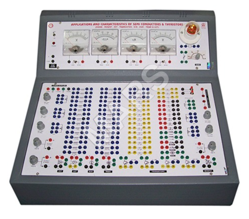
Characteristics & Applications of Basic Thyristors (SCR, DIAC, TRAIC, UJT) (ME 550D)
It is used in scientific industry for various purposes as per the requirements.
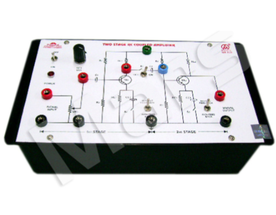
Two Stage RC Coupled Amplifier (ME 619)
Two Stage RC Coupled Amplifier circuit has been designed to study the: A. Voltage Gain & Frequency response of First Stage Amplifier B. Voltage Gain & Frequency response of Second Stage Amplifier C. Voltage Gain & Frequency response of RC Coupled Amplifie
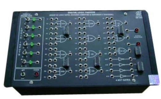
Verification of Booleon Algebra and Demorgan’s Theorems (ME 690)
Verification of Booleon Algebra and Demorgan’s Theorems
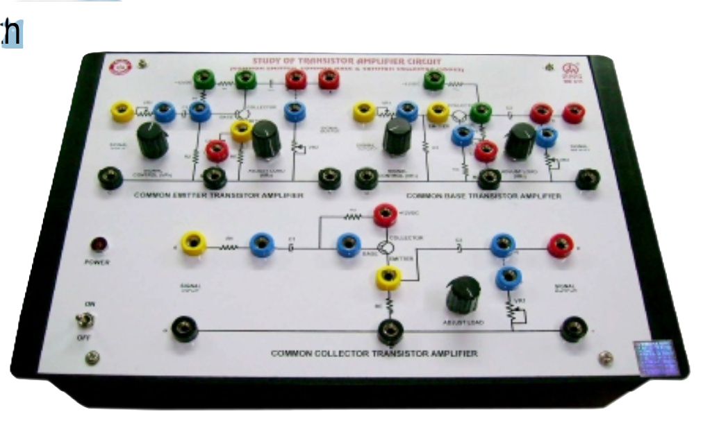
Study of Transistor Amplifier Circuits (With in Common Base, Common Emitter & Common Collector Mode) (ME 611)
Transistor Amplifier Circuits has been designed to plot the frequency response and to measure the following: A. EffectofFeed-Back onoutputinCommonBase&CommonEmitter Amplifier. B. Input Impedance C. Output Impedance D. Band Width E. Gain